


- 询价
- gelatins
- JLC-R10014
- 国产
- 2025年07月15日

10 年钻石会员
企业认证
相关产品推荐更多 >


万千商家帮你免费找货
0 人在求购买到急需产品
- 详细信息
- 技术资料
- 库存:
156
- 英文名:
Molybdenum Disulfide dispersion
- CAS号:
1317-33-5
- 保质期:
6个月
- 供应商:
江西江蓝纯生物试剂有限公司
- 保存条件:
常温干燥避光
中文名称: Graphene Supermarket 二硫化钼分散液
英文名称: Molybdenum Disulfide dispersion
CAS号: 1317-33-5
包 装: 100mL
参 数: 1-8层片径100-400nm 18mg/L
保质期: 6月常温干燥避光
性 质
Lateral Size: 100-400 nm
Thickness: 1-8 monolayers
Purity in dry phase: >99%
Solution Concentration: 18 mg/L
Solution is stable under ambient conditions
应 用
Transistors
Flexible Displays
Optics
MoS2 Research
Inks
Thin Semiconducting Films
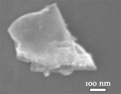
SEM image of an Individual flake
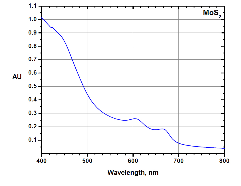
UV-Visible Absorption Spectrum
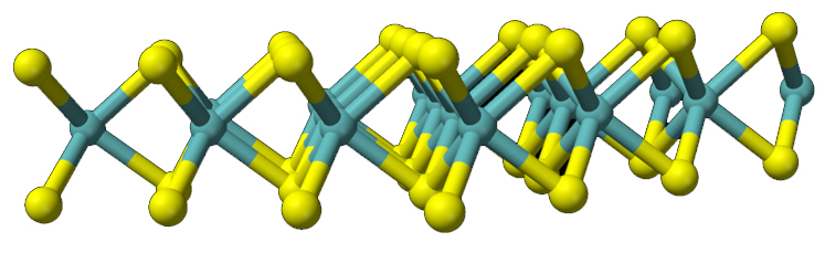
Each Mo(IV) center of MoS2 is occupying a trigonal prismatic coordination sphere, which is bound to six sulfide ligands. The sulfur centre is connected to three Molybdenum centres, which are pyramidal. The trigonal prisms are layered, sandwiching molybdenum atoms between layers of sulfur atoms.
Depiction of MoS2 Crystal Structure1
MoS2 in its monolayer form has recently been under particular recognition for its intriguing electrical and optical properties. Bulk MoS2 is generally an n-type semiconductor with an indirect bandgap (~1.3 eV) and a carrier mobility in the range of 50-200 cm2 V-1s-1 at room temperature. On the other hand, monolayer MoS2 has a direct bandgap of ~1.8 eV, and can be useful in low-power switching devices.
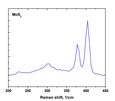
MoS2 Raman Spectrum
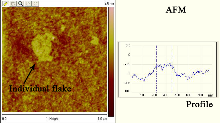
AFM Image of an MoS2 Flake on SiO2
Preparation Method: Solution-Based Exfoliation
This solution can be easily deposited onto a substrate or surface of your choice to form a thin film coating.
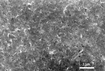
SEM Image of an MoS2 Thin Film on SiO2
英文名称: Molybdenum Disulfide dispersion
CAS号: 1317-33-5
包 装: 100mL
参 数: 1-8层片径100-400nm 18mg/L
保质期: 6月常温干燥避光
性 质
Lateral Size: 100-400 nm
Thickness: 1-8 monolayers
Purity in dry phase: >99%
Solution Concentration: 18 mg/L
Solution is stable under ambient conditions
应 用
Transistors
Flexible Displays
Optics
MoS2 Research
Inks
Thin Semiconducting Films
SEM image of an Individual flake
UV-Visible Absorption Spectrum
Each Mo(IV) center of MoS2 is occupying a trigonal prismatic coordination sphere, which is bound to six sulfide ligands. The sulfur centre is connected to three Molybdenum centres, which are pyramidal. The trigonal prisms are layered, sandwiching molybdenum atoms between layers of sulfur atoms.
Depiction of MoS2 Crystal Structure1
MoS2 in its monolayer form has recently been under particular recognition for its intriguing electrical and optical properties. Bulk MoS2 is generally an n-type semiconductor with an indirect bandgap (~1.3 eV) and a carrier mobility in the range of 50-200 cm2 V-1s-1 at room temperature. On the other hand, monolayer MoS2 has a direct bandgap of ~1.8 eV, and can be useful in low-power switching devices.
MoS2 Raman Spectrum
AFM Image of an MoS2 Flake on SiO2
Preparation Method: Solution-Based Exfoliation
This solution can be easily deposited onto a substrate or surface of your choice to form a thin film coating.
SEM Image of an MoS2 Thin Film on SiO2
风险提示:丁香通仅作为第三方平台,为商家信息发布提供平台空间。用户咨询产品时请注意保护个人信息及财产安全,合理判断,谨慎选购商品,商家和用户对交易行为负责。对于医疗器械类产品,请先查证核实企业经营资质和医疗器械产品注册证情况。
 技术资料
技术资料暂无技术资料 索取技术资料
Graphene Supermarket 二硫化钼分散液
询价