大家都在搜

手机验证

询价列表

暂时没有已询价产品

Graphene Superm
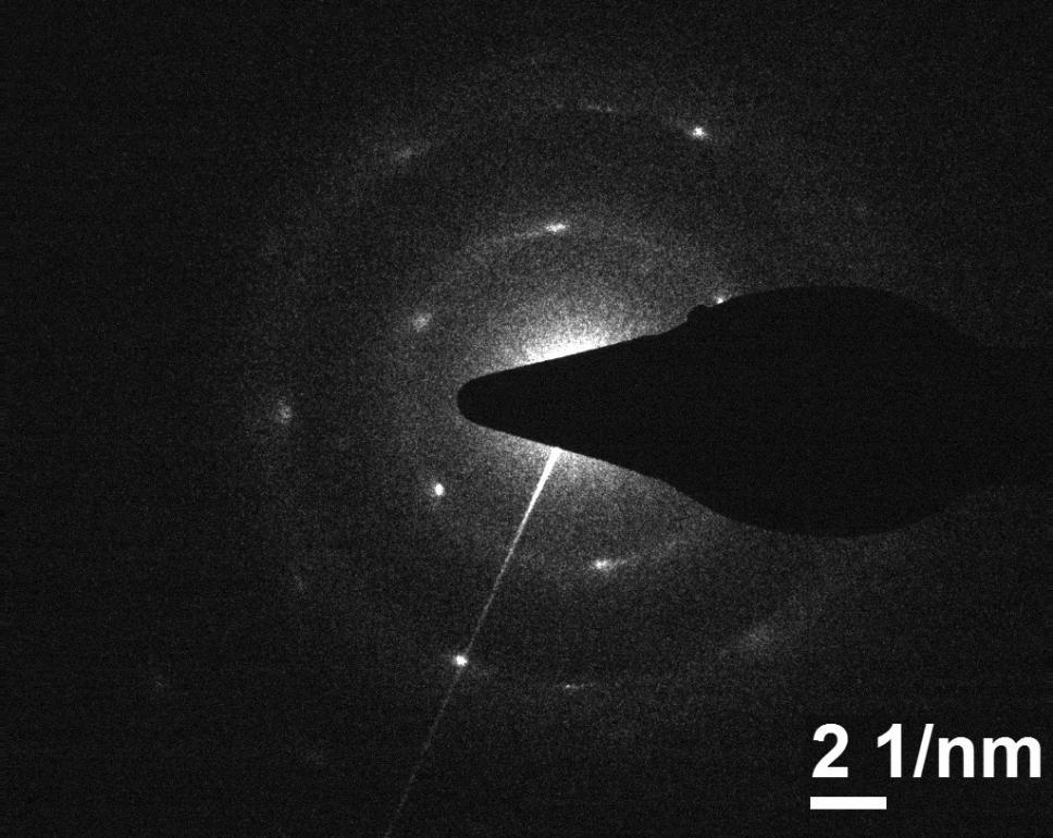
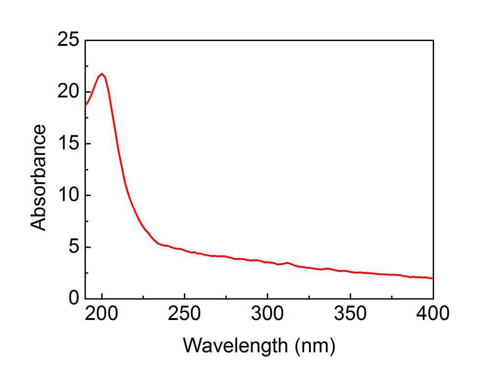
arket铜基六角氮化硼单层薄膜
企业认证
159
Single layer h-BN (Boron Nitride) film grown in copper foil
7440-42-8
6个月
江西江蓝纯生物试剂有限公司
常温干燥避光
1 盒


风险提示:丁香通仅作为第三方平台,为商家信息发布提供平台空间。用户咨询产品时请注意保护个人信息及财产安全,合理判断,谨慎选购商品,商家和用户对交易行为负责。对于医疗器械类产品,请先查证核实企业经营资质和医疗器械产品注册证情况。